

Strain Switches 2D Phase-Change Transistor
25/06/2019 The new technique, which works by applying a voltage-induced strain to a 2D material so that it goes from being a semimetal to a semiconductor, could be used to control devices for ultrafast low-power non-volatile logic and memory.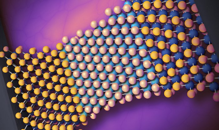
Almost all transistors today rely on the electric-field effect to tune the conductivity of a semiconducting channel from its conducting “on” state to a non-conducing “off” state. As transistors become ever smaller, however, effects such as current leakage become more problematic.
Researchers at the University of Rochester in the US led by Stephen M. Wu have now put forward an alternative to field-effect switching in transistors. Their new technique makes use of electric-field induced strain to control a transistor channel made from a small flake (between 13 to 70 nm thick) of the 2D transition dichalcogenide molybdenum telluride (MoTe2). The MoTe2 flake is deposited on top of a single-crystal oxide substrate, up to 0.3 mm thick, made of the relaxor ferroelectric Pb(Mg1/3Nb2/3)0.71Ti0.29O3 (PMN-PT). This ferroelectric acts as the gate dielectric in the device.
Strain biasing
When the researchers apply a voltage to the gate, this strains the MoTe2 by the converse piezoelectric effect, causing it to stretch. “We use this effect in combination with static thin film stressors to achieve more strain than piezoelectrics or ferroelectrics alone can produce,” explains Wu. “The stretching itself triggers a phase change in the material, so that it goes from being a highly conductive semi-metallic material to a low conductivity semiconducting one. We call this effect ‘strain-biasing’, which allows us to extend the reach of strain-on-a-chip.”
Indeed, the researchers say they can achieve large non-volatile changes in the channel conductivity, Gon/Goff, of around 107 at room temperature with a strain of just 0.4%. To compare, a control device has a Gon/Goff of around 0.04.
“The concept presented in our work combines the best aspects of ferroelectric memory (that is, high-speed, low-power non-volatile operation) with the benefit of having large changes in conductivity at a very steep slope with respect to the applied gate voltage that isn’t limited by the way conventional field-effect transistors function,” says Wu.
More efficient
Normally, the subthreshold swing at which a device changes conductivity with applied gate voltage is limited to 60 mV/dec at room-temperature as a fundamental limit, but our device switches in a different way and so circumvents this problem, he explains. “This allows for much higher ‘on’, and much lower ‘off’, currents, making the device more power efficient,” he tells Physics World.
“Non-volatility also means that we do not have to input additional power to maintain the conductivity state, so this makes the transistor more energy efficient than a conventional device too.”
Low-power, high-speed memory could benefit
The technology could be used anywhere a normal transistor would, but especially in low-power, high-speed memory, he adds. And since the device has the same configuration as a traditional transistor, it could easily be adapted into current electronics – even though much more work is still needed before this can happen. At the moment, the device fails after just 70 to 100 on-off switching cycles.
Wu says he and his colleagues also need to find out how much strain can be applied to MoTe2, and indeed other 2D materials, before it breaks. “The ceiling seems to be high though, since the limits of operation of the individual ferroelectric and phase-change materials are themselves high.”
The researchers, reporting their work in Nature Nanotechnology 10.1038/s41565-019-0466-2, are now busy looking to extend this on-chip strain control of phase in 2D materials to other forms of order.
“There are a huge number of 2D materials out there, and strain could be used to control their optical, magnetic or superconducting properties, as well as their electronic ones,” explains Wu. “This is the ultimate goal of 2D straintronics (devices with unique properties that are engineered through the careful introduction of mechanical deformations in the material): taking all of the properties you couldn’t control before and being able to control them, just by stretching the material on a chip.”
Source: https://bit.ly/2SEvfSk, via Physics World
Conteúdo Relacionado:
GC