

Perovskites A Single Crystal Unit Thick Stand Free
17/06/2019 Perovskites may be the next material to get the full 2D makeover, according to studies by a team of researchers at Nanjing University in China and the University of Nebraska-Lincoln and University of California, Irvine, in the US. While previous work by other researchers had suggested that the crystalline lattice of free-standing perovskites would collapse in films less than five crystal lattice units thick, the researchers led by Peng Wang, Yuefeng Nie and Xiaoqing Pan have now fabricated perovskite in free-standing single unit cell layers.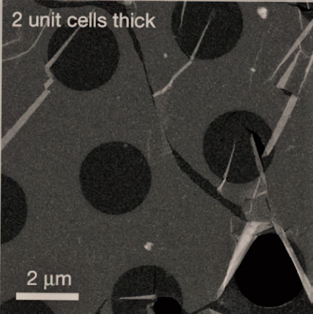
Regular readers of Physics World will already be familiar with perovskites, particularly in our coverage of optoelectronic devices such as solar cells and LEDs, as efficiencies of devices using these materials have skyrocketed in recent years.
They are a class of materials with the formula ABX3, where A and B are metals and X is usually oxygen, and they exist in a number of crystal structures including rhombohedral-like, tetragonal-like, orthorhombic, monoclinic and triclinic phases.
Perovskite studies have already identified a number of attractive properties including high-temperature superconductivity, colossal magnetoresistance, Mott metal–insulator transitions and multiferroicity, and interest in the possibility of identifying new behaviour in 2D forms of the materials has been high. However recent studies by researchers had suggested a practical limit as to how thin films of perovskite could be.
Delicate but stable
To isolate thin perovskite layers Wang, Nie and Pan followed the same procedure that had recently proved successful in other experiments that Harold Y.
Hwang at Stanford University in the US had led. They grew the perovskite on a sacrificial layer of water-soluble Sr3Al2O6 (SAO) and then dissolved the SAO to leave a free-standing perovskite that could then be transferred to a whole range of other substrates, including silicon and holey carbon.
When the team led by Wang, Nie and Pan characterized their free-standing films using TEM using selected-area electron diffraction (SAED) and plan-view and cross-sectional high-angle annular dark-field (HAADF) imaging with atomic resolution they were able to confirm single-crystal phases, even in films just a single crystal unit thick. What they also noticed was that the films were very easily damaged by electron beams, so much so that HAADF measurements on the single layer samples were not possible. However other measurements that did not damage the samples were sufficient for them to draw their conclusions.
The researchers produced free-standing films of both SrTiO3 (STO) a non-polar oxide, and BiFeO3, which has a large ferroelectric polarization pointing through the cells of its rhombohedral lattice in the bulk. In their ultrathin films of STO they observed ripples similar to those seen in graphene, highlighting that while perovskites are brittle in the bulk there may be scope for electronic applications exploiting flexible mechanical properties. Their measurements of BFO films revealed a phase transition from a rhombohedral-like phase as they were grown to a tetragonal-like phase when isolated.
“As useful as graphene”
The isolation of other 2D materials – such as graphene and transition metal dichalcogenides – has revealed a wealth of physics and technological potential that is not apparent from the behaviour of these materials in the bulk. The properties of these 2D materials are largely a result of the s and p orbital electron interactions. In contrast many of the properties that have attracted interest in perovskites so far arise on account of their strongly interacting d orbital electrons, so there are high hopes that isolating 2D perovskites will unearth material behaviour that has not been observed before.
“We anticipate that 2D perovskite oxides could become as useful as graphene in the discovery of unconventional 2D correlated quantum phases,” conclude Wang, Nie and Pan in their report.
They highlight the superconducting properties from twists in bilayer graphene that launched a series of studies into heterostructure twistronics and add that the behaviour of misaligned perovskite sheets remains to be explored. “The ability to transfer any crystalline free-standing perovskite films onto silicon or other semiconducting wafers is likely to enable the direct incorporation of strongly correlated properties in conventional semiconductors, paving the way for a new generation of multifunctional electronic devices.”
Source: https://bit.ly/2LAkBLy, via Physics World
Conteúdo Relacionado:
GC