

Spin Read-out In Atomic qubits In An All-epitaxial Three-dimensional Transistor
27/03/2019 The realization of the surface code for topological error correction is an essential step towards a universal quantum computer. For single-atom qubits in silicon, the need to control and read out qubits synchronously and in parallel requires the formation of a two-dimensional array of qubits with control electrodes patterned above and below this qubit layer.This vertical three-dimensional device architecture requires the ability to pattern dopants in multiple, vertically separated planes of the silicon crystal with nanometre precision interlayer alignment. Additionally, the dopants must not diffuse or segregate during the silicon encapsulation. Critical components of this architecture — such as nanowires, single-atom transistors and single-electron transistors – have been realized on one atomic plane by patterning phosphorus dopants in silicon using scanning tunneling microscope (STM) hydrogen resist lithography.
In our latest work at the Centre for Quantum Computation & Communication Technology (University of New South Wales, Sydney), we extend this STM fabrication technique to three dimensions and demonstrate single-shot spin read-out with 97.9% measurement fidelity of a phosphorus dopant qubit within a vertically gated single-electron transistor with ≤ 5nm interlayer alignment accuracy. Our strategy ensures the formation of a fully crystalline transistor using just two atomic species: phosphorus and silicon.
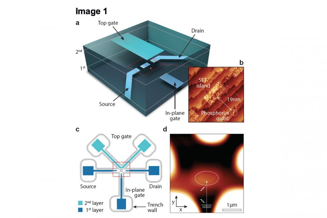
To align two lithographic layers containing device components with respect to each other we pattern our devices on the bottom of wet etched trenches radiating outward from the flat bottom of a central depression. These trenches are etched ~350nm deep using a tetramethylammonium hydroxide etch before terminating with atomic hydrogen as an atomic scale mask for STM hydrogen resist lithography.
The device is positioned at the intersection of the leads in the central region with its micrometer scale contact leads extending along the flat bottomed trenches. By using the centreline of the etched trenches as reference points we can align device structures from one layer to the other. In this way, lithography on the heavily stepped sides of the marker is avoided. In this way we can achieve a ≤5nm interlayer alignment accuracy.
To date precision donor devices have been encapsulated with epitaxial silicon grown at a comparatively low sample temperature of ~250oC needed to minimize P segregation . At such low temperatures mass transport of the Si atoms up and down the step edges is minimal and hence the shape of our alignment markers are only slightly modified during overgrowth. Although the growth is epitaxial, the resulting surface roughness (~1nm) makes lithography on the second plane challenging.
This arises from the comparable height of a single dangling bond (0.17nm) and a Si adatom (0.14nm), where it is difficult to reliably distinguish between the two and validate high quality lithography. Whilst growing at higher substrate temperatures reduces surface roughness it can lead to the segregation of P atoms, especially for temperatures T>400oC, with P desorption occurring at 650oC.
Possible diffusion and segregation of P atoms out of their precision placement therefore limits the thermal budget available for flattening the growth surface. To tackle this problem we exploit an adaptation of kinetic growth manipulation to smoothen the upper surface for a second cycle of STM lithography. The sample is kept at 250oC during most of the encapsulation, but we introduce a rapid thermal anneal sequence (6×1min, 450oC) in the last phase of the growth.
In conventional kinetic growth manipulation anneals are applied to each monolayer of growth to improve surface flatness. Here we adapt this concept to increase the mobility of Si adatoms changing the growth mode from 2D islanding to step-flow growth allowing them to fill up existing vacancies in the lower layers without the diffusion of P. We find the surface roughness (RMS) after growing the encapsulation layer in this way reduces from 0.52±0.15nm to 0.15±0.03nm (Fig. 2b-e). The island size increases from a few atoms to ~100nm2. The flatter surface makes it possible to distinguish single dangling bonds and validate the quality of STM lithograph .
Source:https://bit.ly/2UIt2Zr
via Scienta Omicron