M-2000
J.A. Woollam
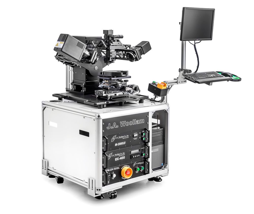
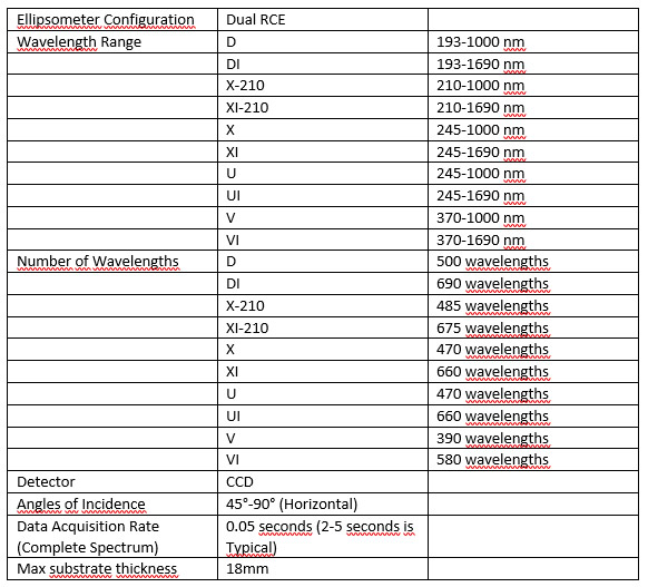
The M-2000® line of spectroscopic ellipsometers is engineered to meet the diverse demands of thin film characterization. An advanced optical design, wide spectral range, and fast data acquisition combine in an extremely powerful and versatile tool. The M-2000 delivers both speed and accuracy. Our patented RCE technology combines Rotating Compensator Ellipsometry with high-speed CCD detection to collect the entire spectrum (hundreds of wavelengths) in a fraction of a second with a wide array of configurations. The M-2000 is the first ellipsometer to truly excel at everything from in-situ monitoring and process control to large-area uniformity mapping and general purpose thin film characterization. No other ellipsometer technology acquires a full spectrum faster.Specifications

Applications
Optical Coatings: Characterize both thickness and refractive index for single- and multi-layer coatings; anti-reflection, high-reflection, or decorative coatings. Calculate the color coordinates for your coating stack under different lighting conditions.Chemistry/Biology: The M-2000 can be used for a variety of chemical and biological applications, either as a stand-alone tool or in combination with one of our many accessories. Study materials under liquid ambient, at high or low temperatures, or in conjunction with QCM-D measurements.
Conductive Organics: Great progress has occurred in the area of organic layers and stacks used for display (OLED) or photovoltaic applications. There are many different materials being studied, from small molecules such as Alq3 to conjugated polymers such as P3HT. Often multiple materials are blended together which requires the wide spectral range of the M-2000 to probe different wavelengths where the organics are optically different. Long-chain molecules may also have significant anisotropy, where orientational stacking of the polymer chains produces different optical constants in different directions.
Semiconductors: Traditional ellipsometry applications are still going strong. Characterize any semiconductor material: resists, photomasks, SiON, ONO stacks, low-k dielectrics, high-k gates, SOI, SiGe, II-VI and III-V ternary and quaternary compounds.
Photovoltaics: Film thickness and optical properties are critical to performance of solar devices. Ellipsometry is used for development and monitoring of all PV materials: a-Si, μc-Si, poly-Si, AR Coatings (SiNx, AlNx ), TCO Films (ITO, ZnOx, doped SnO2, AZO), CdS, CdTe, CIGS, organic PV materials, and dye sensitized films.
In-Situ: The M-2000 is ideal for in-situ monitoring and process control. It is used successfully with a number of different processes to provide real-time results
Options
Focusing Optics

Model (on Fixed or Auto Angle Base)
V, VI 220µm beam dia.
U, UI, D, DI 300µm beam dia.
X, XI 120µm beam dia.
Camera
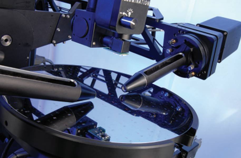
Add a camera to M-2000 systems with focused spot option to visualize the measurement area. The actual beam may not be visible on smooth surfaces, but the location can be identified based on reference location. The camera option includes a 3Mpixel CCD Camera, Lens set, and Illumination setup.
- 3x Magnification
- Field of view: 2.1 x 1.6mm
- Working distance: 77mm
- Digital zoom: up to 8x
Automated Sample Alignment

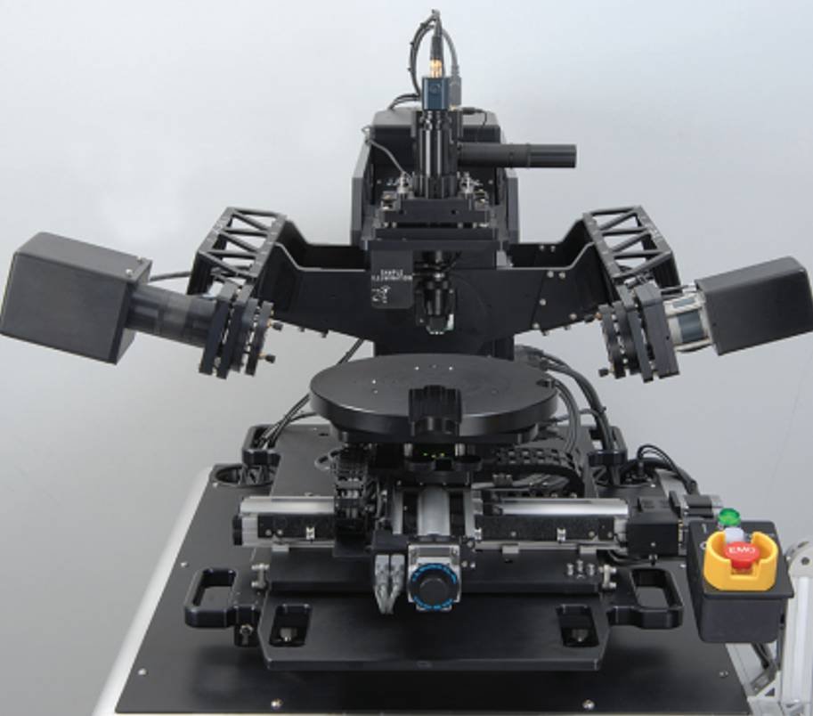
Fully automated sample alignment (tip/tilt and z-height adjustment).


